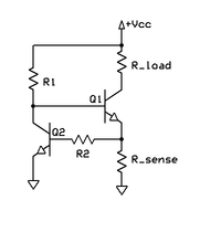
CCS Design - Part 1 (Using two NPN BJT)
Introduction
References
[1] 2N2222 NPN Amplifier Transistor Datasheet - On Semi
Design Notes
1. Rload = 1W White LED
2. Rload current = 100mA
3. Rsense voltage ~= 0.6V
4. Rsense = 0.6V / 100mA
= (0.6 * 1000) / 100
= 6 Ω
6. Rsense power = V * I
= 0.6 * 100mA
= (0.6 * 100) / 1000
= 60 / 1000
= 0.06W
7. IR1 = IRsense / hfe
= 100mA / hFE
~= 100mA / 100
~= 1mA
8. R1 = (Vcc - Vb1 - Vbe2) / IR1
= (12V - (0.6V + 0.6V) ) / 1mA
~= 10.8V / 1mA
~= 11kΩ
~= 10kΩ
Appendices
Appendix A - Constant current source with thermal compensation - Wikipedia
Current source
One limitation with the circuits in Figures 5 and 6 is that the thermal compensation is imperfect. In bipolar transistors, as the junction temperature increases the Vbe drop (voltage drop from base to emitter) decreases. In the two previous circuits, a decrease in Vbe will cause an increase in voltage across the emitter resistor, which in turn will cause an increase in collector current drawn through the load. The end result is that the amount of 'constant' current supplied is at least somewhat dependent on temperature. This effect is mitigated to a large extent, but not completely, by corresponding voltage drops for the diode, D1, in Figure 6, and the LED, LED1, in Figure 5. If the power dissipation in the active device of the CCS is not small and/or insufficient emitter degeneration is used, this can become a non-trivial issue.
Imagine in Figure 5, at power up, that the LED has 1 V across it driving the base of the transistor. At room temperature there is about 0.6 V drop across the Vbe junction and hence 0.4 V across the emitter resistor, giving an approximate collector (load) current of 0.4/Re amps. Now imagine that the power dissipation in the transistor causes it to heat up. This causes the Vbe drop (which was 0.6 V at room temperature) to drop to, say, 0.2 V. Now the voltage across the emitter resistor is 0.8 V, twice what it was before the warmup. This means that the collector (load) current is now twice the design value! This is an extreme example of course, but serves to illustrate the issue.
The circuit to the left overcomes the thermal problem (see also, current limiting). To see how the circuit works, assume the voltage has just been applied at V+. Current runs through R1 to the base of Q1, turning it on and causing current to begin to flow through the load into the collector of Q1. This same load current then flows out of Q1's emitter and consequently through Rsense to ground. When this current through Rsense to ground is sufficient to cause a voltage drop that is equal to the Vbe drop of Q2, Q2 begins to turn on. As Q2 turns on it pulls more current through its collector resistor, R1, which diverts some of the injected current in the base of Q1, causing Q1 to conduct less current through the load. This creates a negative feedback loop within the circuit, which keeps the voltage at Q1's emitter almost exactly equal to the Vbe drop of Q2. Since Q2 is dissipating very little power compared to Q1 (since all the load current goes through Q1, not Q2), Q2 will not heat up any significant amount and the reference (current setting) voltage across Rsense will remain steady at ≈0.6 V, or one diode drop above ground, regardless of the thermal changes in the Vbe drop of Q1. The circuit is still sensitive to changes in the ambient temperature in which the device operates as the BE voltage drop in Q2 varies slightly with temperature.
.END


Comments
Post a Comment